![]() Tips for schematic editor, Composer
Tips for schematic editor, Composer
![]() Prerequisite:
Already go through the tutorial mentioned in the last section.
Prerequisite:
Already go through the tutorial mentioned in the last section.
Now, you already know how to draw a schematic and have a symbol for it. But is there anything not mentioned in the tutorial? Yes. The followings are some tips for you.
![]() I cannot download the model file from MOSIS, is there any default model file in
CAE?
I cannot download the model file from MOSIS, is there any default model file in
CAE?
![]() Yes, but I will recommend you download the model file from your instructor if
provided, or download it from here. Just like what you did
in HSpice, you need to know the model name from NMOS and PMOS. (Don't know, just
open the model file! Then you would see the name following .model) When you want
to insert the NMOS, PMOS, or other components, please insert from 'analogLib',
and choose 'active->nmos4 or pmos4'. In the 'model name' field, fill in the
model name you just saw in the file and assign the required value like width,
length, etc. You don't need to fill in all the field because Spectre will
calculate the other field that you didn't give the value. For other component,
like capacitor or resistor, you could click on 'Passives' for the library name,
fill in the value for them, then paste them on your schematic.
Yes, but I will recommend you download the model file from your instructor if
provided, or download it from here. Just like what you did
in HSpice, you need to know the model name from NMOS and PMOS. (Don't know, just
open the model file! Then you would see the name following .model) When you want
to insert the NMOS, PMOS, or other components, please insert from 'analogLib',
and choose 'active->nmos4 or pmos4'. In the 'model name' field, fill in the
model name you just saw in the file and assign the required value like width,
length, etc. You don't need to fill in all the field because Spectre will
calculate the other field that you didn't give the value. For other component,
like capacitor or resistor, you could click on 'Passives' for the library name,
fill in the value for them, then paste them on your schematic.

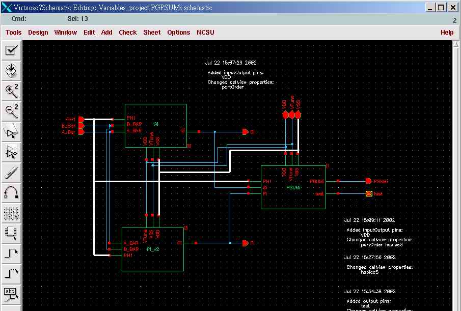
![]() How to check the connection status of your design?
How to check the connection status of your design?
![]() Let's assume you have a big design and after the simulation, you know there is
something wrong with your design, then is there any function that you could
check? The answer is yes. Now following the steps below,
Let's assume you have a big design and after the simulation, you know there is
something wrong with your design, then is there any function that you could
check? The answer is yes. Now following the steps below,
(1) Find a wire which you want to check
(2) Click the right bottom several times, two or three times, very quickly on this wire
(3) The white lines are those wires which is connected to this wire

If you want to check two different wires at the same time, after checking the first wire, press 'Shift' on your keyboard to select this new wire, release the 'Shift' and then do the steps 1. Sometimes you fail, but try more times then you could get the way.
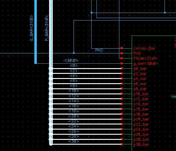
![]() Can I connect two buses with different number of pins?
Can I connect two buses with different number of pins?
![]() Theoretically, yes. But there is a restriction for this. The two buses should
not contain one or above useless pin among the bus. i.e., should be <31:0>
to <30:0>. If there is a useless pin, let's say pin 23 in <30:0> and
<31:0>, you have to connect <31:24> to <30:24> (pin 31 is
floating), then connect <22:0> to <22:0>.
Theoretically, yes. But there is a restriction for this. The two buses should
not contain one or above useless pin among the bus. i.e., should be <31:0>
to <30:0>. If there is a useless pin, let's say pin 23 in <30:0> and
<31:0>, you have to connect <31:24> to <30:24> (pin 31 is
floating), then connect <22:0> to <22:0>.
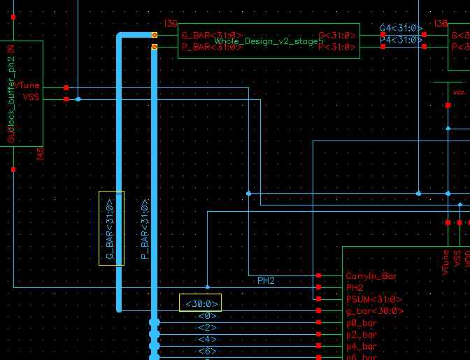
If there are lots of gaps among the bus, you have better split one of the bus and then connect it like the followings
![]() How can I print out my design?
How can I print out my design?
![]() It's very easy to print out your design. However, there are still something you
need to know.
It's very easy to print out your design. However, there are still something you
need to know.
How to print? Click on Design->Plot->Submit
![]()
Then another window will pop-up. In this window, be sure to check the total pages that will be printed out. The default in Composer is the 1:1 mapping to the Letter Size paper, which means if your design is very large, the number of pages printed will also increase. If you want to fit your design into only one page, be sure to click on "Plot Option" and then choose "fit to page".
![]()
![]()
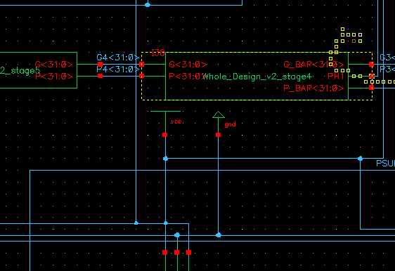
![]() Where is the voltage source and ground symbol?
Where is the voltage source and ground symbol?
![]() There are lots of voltage sources and ground symbols you could choose. Some of
them are in the library, analogLib. The instances, vcc and gnd, are what I use
very often. Remember, be sure to add a 'vcc' in your top-level schematic because
if you forget to add it, you might not assign the value of 'vcc' when
simulating.
There are lots of voltage sources and ground symbols you could choose. Some of
them are in the library, analogLib. The instances, vcc and gnd, are what I use
very often. Remember, be sure to add a 'vcc' in your top-level schematic because
if you forget to add it, you might not assign the value of 'vcc' when
simulating.
![]() I
want to tune the bulk voltage. However, when I add a ''vcc', I cannot see the
port on the symbol, what could I do?
I
want to tune the bulk voltage. However, when I add a ''vcc', I cannot see the
port on the symbol, what could I do?
Tuning the size of transistor is very important issue, but how could we do? As you know, it is different from the voltage source. The best way to solve it is adding a 'InputOutput' port by clicking 'p' and choose 'InputOutput' for this port. Then this port will appear on the top of the symbol and then you could connect it in the top-level.

![]() Oh, gosh, my windows are frozen, what can I do?
Oh, gosh, my windows are frozen, what can I do?
![]() Once your windows are frozen or crashed, the way I found to recover it is
to restart composer again and open the design. At this time, your design may
beread only and if you decide to return to the edit mode, first, go to the
terminal window, change directory to 'your_design/schematic/' then you will see
a file, called, 'sch.cdb.cdslck', delete this file then you could edit your
design again. However, this only return to the last saved design.
Once your windows are frozen or crashed, the way I found to recover it is
to restart composer again and open the design. At this time, your design may
beread only and if you decide to return to the edit mode, first, go to the
terminal window, change directory to 'your_design/schematic/' then you will see
a file, called, 'sch.cdb.cdslck', delete this file then you could edit your
design again. However, this only return to the last saved design.